- 您现在的位置:买卖IC网 > Sheet目录234 > MAX14541EAXK+T (Maxim Integrated Products)IC ESD PROTECTOR 3CH SC70-5
�� �
�
�3-Channel,� Low-Leakage� ESD� Protector�
�________________Detailed� Description�
�The� MAX14541E� low-leakage,� low-capacitance,� Q� 15kV�
�ESD-protection� diode� arrays� are� suitable� for� high-speed�
�and� general-signal� ESD� protection.� Low� input� capaci-�
�tance� makes� this� device� ideal� for� ESD� protection� of�
�high-speed� signals.� Each� channel� consists� of� a� pair� of�
�diodes� that� steer� ESD� current� pulses� to� V� CC� or� GND.� The�
�MAX14541E� is� a� 3-channel� device� (see� the� Functional�
�Diagram� ).�
�The� MAX14541E� is� designed� to� work� in� conjunction� with�
�a� device’s� intrinsic� ESD� protection.� The� MAX14541E�
�limits� the� excursion� of� the� ESD� event� to� below� Q� 25V�
�peak� voltage� when� subjected� to� the� Human� Body� Model�
�waveform.� When� subjected� to� the� IEC� 61000-4-2� Contact�
�Discharge� waveform,� the� peak� voltage� is� limited� to�
�Q� 60V.� The� peak� voltage� is� limited� to� Q� 100V� when� sub-�
�jected� to� Air-Gap� Discharge.� The� device� protected� by�
�the� MAX14541E� must� be� able� to� withstand� these� peak�
�voltages,� plus� any� additional� voltage� generated� by� the�
�parasitic� of� the� board.�
�___________Applications� Information�
�Design� Considerations�
�Maximum� protection� against� ESD� damage� results� from�
�proper� board� layout� (see� the� Layout� Recommendations�
�section).� A� good� layout� reduces� the� parasitic� series�
�inductance� on� the� ground� line,� supply� line,� and� protect-�
�ed� signal� lines.� The� MAX14541E� ESD� diodes� clamp� the�
�voltage� on� the� protected� lines� during� an� ESD� event� and�
�shunt� the� current� to� GND� or� V� CC� .� In� an� ideal� circuit,� the�
�clamping� voltage� (V� C� )� is� defined� as� the� forward� voltage�
�drop� (V� F� )� of� the� protection� diode,� plus� any� supply� volt-�
�age� present� on� the� cathode.�
�For� positive� ESD� pulses:�
�V� C� =� V� CC� +� V� F�
�For� negative� ESD� pulses:�
�where� I� ESD� is� the� ESD� current� pulse.�
�During� an� ESD� event,� the� current� pulse� rises� from� zero�
�to� peak� value� in� nanoseconds� (Figure� 2).� For� example,�
�in� a� +15kV� IEC� 61000-4-7� Air-Gap� Discharge� ESD� event,�
�the� pulse� current� rises� to� approximately� 45A� in� 1ns�
�(di/dt� =� 45� x� 10� 9� ).� An� inductance� of� only� 10nH� adds� an�
�additional� 450V� to� the� clamp� voltage,� and� represents�
�approximately� 0.5in� of� board� trace.� Regardless� of� the�
�device’s� specified� diode� clamp� voltage,� a� poor� layout�
�with� parasitic� inductance� significantly� increases� the�
�effective� clamp� voltage� at� the� protected� signal� line.�
�Minimize� the� effects� of� parasitic� inductance� by� placing�
�the� MAX14541E� as� close� as� possible� to� the� connector�
�(or� ESD� contact� point).�
�A� low-ESR� 0.1� F� F� capacitor� is� required� between� V� CC� and�
�GND� to� get� the� maximum� ESD� protection� possible.� This�
�bypass� capacitor� absorbs� the� charge� transferred� by� a�
�positive� ESD� event.� Ideally,� the� supply� rail� (V� CC� )� would�
�absorb� the� charge� caused� by� a� positive� ESD� strike�
�without� changing� its� regulated� value.� All� power� supplies�
�have� an� effective� output� impedance� on� their� positive�
�rails.� If� a� power� supply’s� effective� output� impedance� is�
�1� I� ,� then� by� using� V� =� I� x� R,� the� clamping� voltage� of� V� C�
�increases� by� the� equation� V� C� =� I� ESD� x� R� OUT� .� A� +8kV� IEC�
�61000-4-2� ESD� event� generates� a� current� spike� of� 24A.�
�The� clamping� voltage� increases� by� V� C� =� 24A� x� 1� I� ,� or�
�V� C� =� 24V.� Again,� a� poor� layout� without� proper� bypassing�
�increases� the� clamping� voltage.� A� ceramic� chip� capaci-�
�tor� mounted� as� close� as� possible� to� the� MAX14541E�
�V� CC� pin� is� the� best� choice� for� this� application.� A� bypass�
�capacitor� should� also� be� placed� as� close� as� possible� to�
�the� protected� device.�
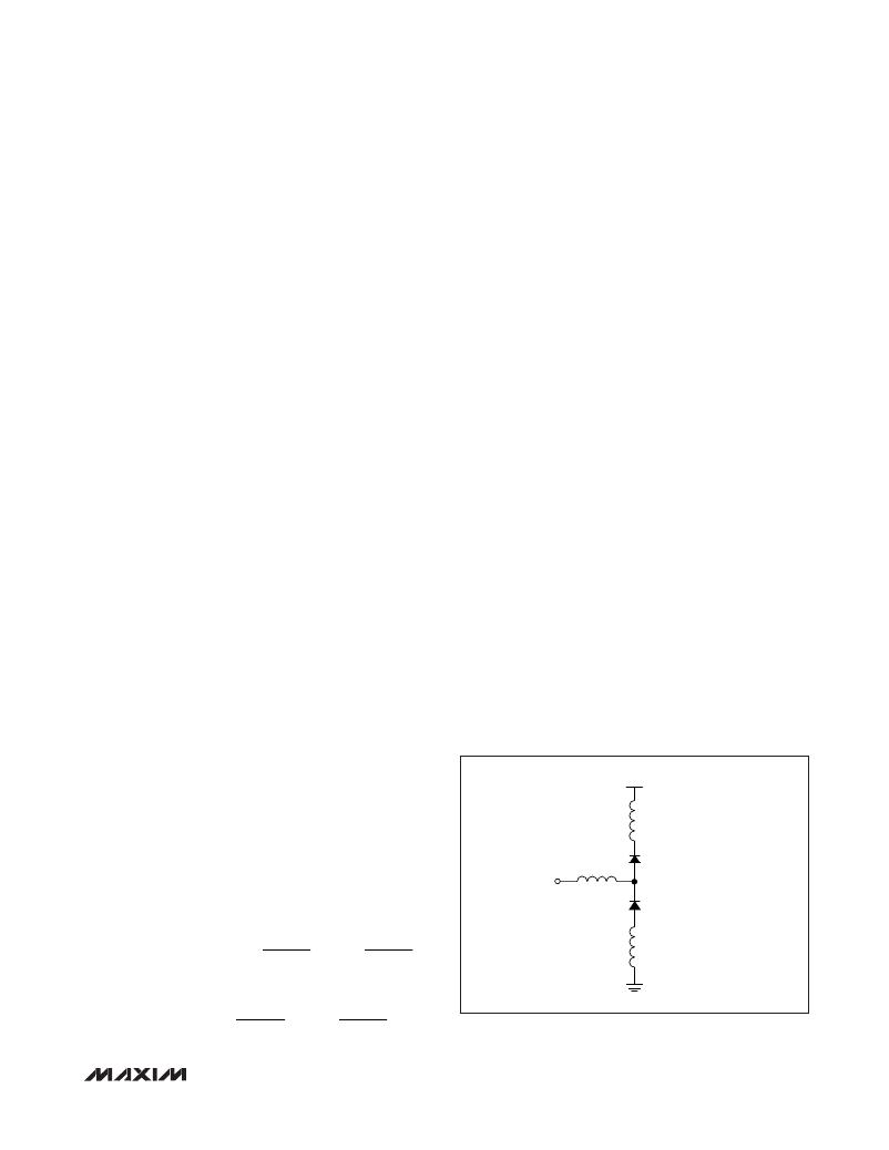
�POSITIVE� SUPPLY� RAIL�
�L2�
�V� C� =� -V� F�
�The� effect� of� the� parasitic� series� inductance� on� the� lines�
�must� also� be� considered� (Figure� 1).�
�For� positive� ESD� pulses:�
�PROTECTED�
�LINE�
�L1�
�D1�
�I/O_�
�D2�
�d� (� I� ESD� )� ?� ?�
�?� +� ?� L2� �
�?� ?�
�d(I� ESD� )� ?�
�?�
�?�
�V� C� =� V� CC� +� V� F(D1)� +� ?� L1� �
�?�
�For� negative� ESD� pulses:�
�dt�
�dt� ?�
�L3�
�GROUND� RAIL�
�V� C� =� ?� ?� V� F(D2)� +� ?� L1� � +� ?� L3� �
�?�
�?�
�d(I� ESD� )� ?� ?�
�?� ?�
�?� ?� d(I� ESD� )� ?� ?�
�?� dt� ?� ?�
�dt� ?� ?�
�Figure� 1.� Parasitic� Series� Inductance�
�_______________________________________________________________________________________�
�5�
�发布紧急采购,3分钟左右您将得到回复。
相关PDF资料
MAX3204EETT+T
IC ESD PROT ARRAY 6-TDFN
MAX3205EATE+
IC ESD PROT DIFF 16-TQFN
MAX5490GA01000+T
RES NET 50K OHM 2 RES SOT23-8
MAX5491NA01500+T
RES NET MULT OHM 2 RES SOT-23
MAX5492LB10000+T
RES NET MULT OHM 2 RES SOT-23
MB2181SS2G13-CC
SWITCH PUSH 4PDT 0.4VA 28V
MB2185SB1W01-6C-A
SWITCH PUSHBUTTON 4PDT 6A 125V
MB2411JA01-G-1A
SWITCH PUSHBUTTON SPDT 3A 125V
相关代理商/技术参数
MAX14544ETA+
制造商:Maxim from Components Direct 功能描述:MAXIM MAX14544ETA+ CURRENT LIMITING SWITCHES - Boxed Product (Development Kits) 制造商:Maxim 功能描述:Maxim MAX14544ETA+ Current Limiting Switches
MAX14544ETA+T
功能描述:电源开关 IC - 配电 ILIM VBUS Accessory Switch RoHS:否 制造商:Exar 输出端数量:1 开启电阻(最大值):85 mOhms 开启时间(最大值):400 us 关闭时间(最大值):20 us 工作电源电压:3.2 V to 6.5 V 电源电流(最大值): 最大工作温度:+ 85 C 安装风格:SMD/SMT 封装 / 箱体:SOT-23-5
MAX14544EVKIT+
功能描述:模拟开关 IC 28V-Capable ILIM VBUS Accessory Switch RoHS:否 制造商:Texas Instruments 开关数量:2 开关配置:SPDT 开启电阻(最大值):0.1 Ohms 切换电压(最大): 开启时间(最大值): 关闭时间(最大值): 工作电源电压:2.7 V to 4.5 V 最大工作温度:+ 85 C 安装风格:SMD/SMT 封装 / 箱体:DSBGA-16
MAX14545ETA+T
制造商:Maxim Integrated Products 功能描述:28V-CAPABLE ILIM VBUS ACCESSORY SWITCH - Tape and Reel
MAX14547AEUT+
制造商:Rochester Electronics LLC 功能描述: 制造商:Maxim Integrated Products 功能描述:
MAX14547AEUT+T
制造商:Rochester Electronics LLC 功能描述: 制造商:Maxim Integrated Products 功能描述:
MAX14548AEEWL+T
制造商:Maxim Integrated Products 功能描述:100MBPS, 16-CHANNEL LLTS - Tape and Reel
MAX14548EEVKIT+
制造商:Maxim Integrated Products 功能描述:16 CHANNEL LLT - Boxed Product (Development Kits)